TP-Link EAP Flash SPI extraction and investigation (using the Hardsploit)
Konstantinos Xynos
Tuesday, June 18, 2019
Introduction
In this post I will be looking at the TP-LINK EAP 110 and what can be extracted from the SPI Flash chip (i.e., local storage). I will demonstrate what can be found, analysed and where the DES key is stored.WARNING: Proceed with caution when doing any hardware and software (i.e. like re-flashing, changes to firmware and uploading it etc). I can't be held liable for anything you do as a result of this post and/or damage that may occur. This is just an educational post.
TP-LINK EAP hardware
Hardware used:
- Pomona type clip
- Hardsploit v1.1(link)
- TP-Link EAP 110
 |
| Fig. 1. TP-Link EAP 110 - SPI flash |
 |
| Fig. 2. Pomona IC test clip 8 pin |
In this case, the device can be extracted using a POMONA IC test clip 8 pins (e.g. example or fig. 2.) and I will viper (i.e., place clip on top) onto the SPI flash. At this stage you have to be very careful not to make any errors. Make sure and double check where pin 1 is and to wire up the voltage correctly. If done incorrectly you will end up burning your chip and board, and possibly any thing else too. Voltage pins are not always required, but if you do need to power the target board be very careful.
Make sure to read the SPI flash chips documentation. This is in the form of the datasheet (e.g. GD25Q64C ext. link). It will include a lot of the hardware and software details needed to talk to the chip. Things to look out for and make a note of: command op codes (i.e., Read 0x03, manufacturer ID 0x90), maximum voltage, maximum operating frequency, chip size, page size, pin layout (i.e., standard SPI pins compared to dual or quad), timing details as graphs, any security considerations (i.e., write protect), memory layout etc.
WARNING: Always make sure that the voltage of the SPI flash chip is rated the same as the output pins of the device that you are using.
The Hardsploit provides the ability for the user to pick the output voltage of the pins. Make sure it is correct and compatible. If the chip supports 3.3 volts then ensure the kit is set to 3.3 volts or ensure that the kit doesn't output more. Usually you can tell or quickly test it with the Saleae Pro voltage view.
Wiring and setup
Wiring tends to be very standard with SPI flash chips, at least the handful ones I have seen. Always double check in case it is different with the particular manufacturer. But overall the layout remains the same across manufacturers, but double check!Here is an example of the wiring of the SPI flash chip I am looking at in this post.
 |
| Fig. 3. SPI Flash - 8 pin |
Within the Hardsploit application it is possible to define the layout of the chip (fig. 3. and 5.) and this will then indicate which I/O pin on the Hardsploit corresponds to which pin on the SPI chip. These will be one-to-one direct connections. So when it says SO it will map to a SO pin (chip or target board). Check the next section for detailed instructions on wiring the chip with the Hardsploit.
Read the whole article before you begin any wiring. Usually completing the configuration of the Hardsploit will help before starting to wiring it all up.
I tend to have my Hardsploit unplugged from the USB port, while I complete the wiring with the target board. This ensures that, if I am applying my own power, I am not shorting any unwanted pins with the Pomona clip. Not applying power straight away also allows me to ensure that the wiring is correct before powering it all on. At this point I go over all the wiring just in case I missed something.
Once I am sure all the wiring is correct, I can plug in the Hardsploit to the computer and I can start the associated application (i.e. hardsploit_gui). If you are powering the target board using the Hardsploit then you will notice the target board lighting up, very faintly. This tends to be a good sign and you should extract the SPI flash as fast as possible, before any changes occur to it.
When I have completed the extraction, I tend to remove the USB cable from the Hardsploit or computer as a way to power down the system.
Extracting the firmware (hardware)
To plug and unplug the Hardsploit from the target device, see the previous section. |
| Fig. 4. Hardsploit - add chip component |
Without any wiring to the target device yet plug in the Hardsploit to the computer and start up the GUI interface hardsploit_gui. On the right at the bottom of the available chips (fig. 9.) there is a create component. From there you can add a new SPI flash chip, and not only (fig. 4.).
 |
| Fig. 5. Hardsploit - chip setup |
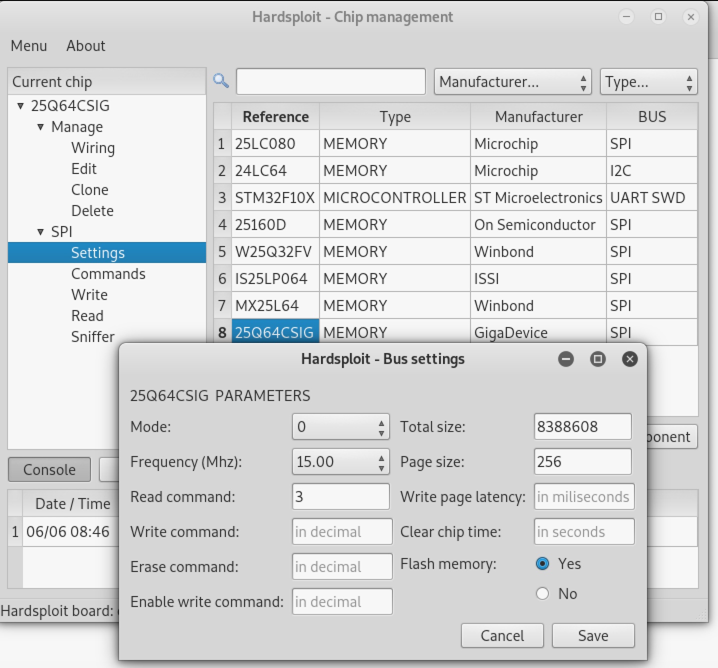
Provide a name and a description. Select the appropriate voltage, mine is 3.3v. Select a manufacturer. GigaDevice is not in the default database so I add it in the Other field. I then select MEMORY as a type and TSOP as the package. These will be important for the wiring later on. Next we will define the pin layout as defined in the manual provided by the manufacturer. Select SPI under Bus and then a few SPI signals will appear under Signal (fig. 4 and 5). Feel free to use the NA if something is not used or as a placeholder (i.e., to show that you completed the wiring).
Under Settings I will setup the Mode as 0, the Read Command as 0x3, the frequency 15Mhz, the total size 8388608 and the page size 256 (fig. 6).
 |
| Fig. 6. Hardsploit - chip settings |
Sometimes you might need to vary the frequency to get the anticipated results. I found the 15Mhz worked just fine for this chip.
Once the setup is complete you will need to find out what the wiring is from the Hardsploit board for each pin. Under Wiring, a window will present the SPI chip and by selecting the mapped out chip legs (fig. 7.) a light on the Hardsploit board will light up (fig. 8.). This pin will map out to the SPI flash pin or Pomona clip.
 |
| Fig. 7. Hardsploit - Example of wiring selection and pin light up (different chip) |
When you have finished the wiring you can then plug into the target device, as I mentioned before. That is, unplug the Hardsploit from the computer, clip onto the SPI flash chip and then provide connectivity and power by plugging in the Hardsploit back into the computer. You might need to restart the GUI application.
 |
| Fig. 8. Hardsploit - wiring light up of SPI pin 1 (NB, might differ based on setup) |
If everything is up and running you should now be able to select the SPI Chip (Current chip) and then select Read. Provide an appropriate file name, Full Read and Read to start the process (fig. 9.).
 |
| Fig. 9. Hardsploit - Read file |
You can verify the extraction process by having a quick look using the hexdump command. You should see some hex values instead of all 0x0.
hexdump -C filename.bin | more
Firmware analysis (software)
There are a number of ways that you can approach this task. Since I had access to the device is was easy for me to check what was available to me from within the OS. Within the Web admin, I enabled SSH access and then connected to the Access Point. It seems that uclited provides you with a lot of information and functionality (i.e., /usr/bin/uclited -p). In figure 10, you can see the partition tables of the flash as mapped out. These are identical to those of the dumped flash chip. Enjoy!
 |
| Fig. 10. Partition locations and sizes via uclited |
Researchers have found the symmetric key and managed to decrypt the exported configuration. This gave me the idea that the configuration stored in the SPI flash chip would also be encrypted. I would therefore need to extract it. Again, there are a number of ways to extract the configuration. You could automate it.
Extract the user configuration
The configuration is stored at position 0x7C0000 (8126464 decimal) and has a size of 0x10000 (65536 decimal), fig. 10. There is also a header which I will remove as it is not needed for the extraction process. You can look into it if you like. The extra header info 152 bytes (0x98 bytes) in size. So we add to the offset (0x7C0000+0x98=0x7C0098) and subtract from the size (0x10000-0x98=0xFF68).
New offset is: 0x7C0098 (8126616 bytes)
New size is : 0xFF68 (65384 bytes)
$ dd if=extracted-flash.bin of=config.bin skip=8126616 count=65384 bs=1
The next thing that is required is the decryption of the config section. As I mentioned before, there is work that was carried out by teknoraver.net (link) that I came across and details how they found the key. The decryption key is 478DA50BF9E3D2CF. I did my own investigation, you can find it in the next section. Decoding can be achieved in a number of ways, one that works in Linux and Mac OS involves using OPENSSL, the command follows:
$ openssl enc -d -des-ecb -K 478DA50BF9E3D2CF -nopad -in config.bin -out config.lztp
Once decoded I end up with a zlib file. You can check this by looking for the zlib magic numbers (RFC 1950), which are 789C. If you run binwalk it should report that a zlib section has been detected. Extraction is completed with the -e flag:
$ binwalk -e config.lztpIf you want to look into zlib process that TP-Link use there is a small conversation at this link.
I have not gone into depth with analysing the Operating System's files. These can be eassily dumped using binwalk over the OS section.
Reversing to find the config DES key
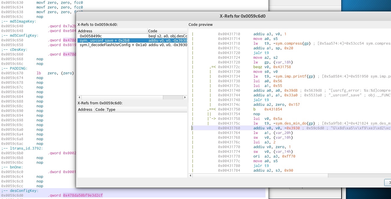
Software used: Cutter (radare2)I managed to do some reversing of the binaries (extracted from above) in order to find where the DES key is being used. Initially, I did a grep to find which application would have the DES key. I was lucky and found that key was in the executable uclited.
 |
| Fig. 11. The DES key as found in uclited |
The same key is used in a number of areas and functions. As can be seen in fig. 11. the location of the DES key is shown. From there I used xfers (e.g., track which functions make calls to the address) which showed two interesting functions that relate to the user configuration, fig. 12.
 |
| Fig. 12. The DES key as found in uclited with the two functions that use it. |
Device Forensics
I have demonstrated how to dump and extract the user configuration from the TP-Link EAP 110.The configuration contains the configured username, password of the system, the APs and WPA/WAP2 passphrases used and any other possible configurations.
There was no log data found.
Since this post has become so large I will make a separate post about any other possible forensic artefacts that can be extracted from the system.
Conclusions
I can honestly say that I am really impressed with the ability of Hardsploit to dump a wide variety of SPI flash chips, especially when dealing with in system programming (ISP), i.e. those SPI chips that are still on board. It is great to be able to extract a chip's contents with minimal damage and interference to the circuit.The reason this post makes use of the Hardsploit is because I have tried other types of boards and found that the Hardsploit tends to be the most reliable and with the best results every time. At least for me, and I have analysed quite a few boards and chips which have not made it to a blog post. Maybe I should make a list of chips I have dumped using the Hardsploit as a live document and testament to its versatility. Other types of devices I have used or attempted to extract SPI chip devices in-circuit included: The Shikra, Buspirate and a Raspberry Pi. These are not always successful in dumping anything in ISP mode.
What is interesting with routers and Access Points is how easy it is to access them and dump the SPI chips using the Hardsploit and Pomona clips.
Labels: firmware extraction, forensics, main, router, tp-link, tplink, weak password hash
Post a Comment